The telescopic implementation could not preserve the required swing at 1.0 V, so the OTA moved to a PMOS-input folded cascode.
← Home
RD-001
Third-order feedforward 3‑bit ΣΔ modulator
A low-voltage redesign of a published third-order feedforward architecture, implemented and simulated in the Cadence GPDK045 generic PDK at 1.0 V. Limited headroom and sampling-switch overdrive led to a folded-cascode OTA, bootstrapped sampling, and resistive CT-CMFB.
Verification snapshot
- Technology / supply
- GPDK045 · 1.0 V
- Noise-included behavioral SNDR
- 78.38 dB mean20 independent noise realizations · range 78.05–78.81 dB
- Behavioral ENOB
- 12.73 bitmean over the same noise realizations
- Partial power estimate
- ≈46 µW≈40 µW VDD core + 6.25 µW DAC ladders
SNDR and ENOB use a behavioral model whose DAC scaling remains unverified. Power is a partial estimate. Verification scope.
What changed at 1.0 V
The feedforward loop topology stayed intact. At 1.0 V, the limiting issues were OTA headroom, sampling-switch gate drive, and common-mode control.
A supply-driven gate loses overdrive as the sampled signal rises. Near mid-supply, VGS is only 0.50 V against an extracted VTH,N of 0.588 V, leaving inadequate strong-inversion drive and a signal-dependent on-resistance.
SC-CMFB inherits the same low-voltage switching problem, so common-mode control was moved to a resistive continuous-time loop.
Starting architecture: the published 180 nm, 1.8 V third-order feedforward design. This work retains its loop topology and redesigns the circuit blocks for 1.0 V.
System architecture
Simplified single-ended signal-flow view.
Swipe horizontally to inspect full signal flow →
Three cascaded DS-SC integrators feed a summing node and 3-bit flash quantizer. A resistive DAC closes the loop.
Differential signal pairs shown single-ended for clarity.Three circuit decisions at 1.0 V
The loop topology stayed the same. The OTA, sampling switch, and common-mode path changed for specific low-voltage reasons.
OTA
PMOS-input folded-cascode OTA
The telescopic stack did not preserve the required headroom at 1.0 V. A PMOS-input folded cascode was used instead, with the final schematic reaching 47.6 dB DC gain, 13.0 MHz GBW, and 89.4° phase margin. The 13.0 MHz AC result uses a 500-fF load. The paper adopts a 9-bit integrator-settling criterion, not full 13-bit settling. Its first-stage calculation gives a 5.7% nominal bandwidth margin before actual non-overlap timing is established.
- DC GAIN
- 47.6 dB
- GBW
- 13.0 MHz
- PHASE MARGIN
- 89.4°
- CORE POWER
- ≈2.3 µW

SAMPLING SWITCH
FIXED GATE DRIVEVGS falls as VIN rises
BOOTSTRAPPED GATE DRIVEVGS ≈ 1.0 V
Dessouky-Kaiser bootstrapped switch
The design problem is insufficient and signal-dependent gate overdrive, which raises and modulates on-resistance across the input range. A 50-fF bootstrap capacitor keeps VGS,MNSW near the 1.0-V supply, reducing that signal dependence. The schematic gives Ron ≈ 2.57 kΩ for the 120-nm main switch.
V
GS,MNSW
≈ V
DD
R
on
= 2.57 kΩ
W
MNSW
= 120 nm

Resistive continuous-time CMFB
SC-CMFB would reuse switches subject to the same low-voltage gate-drive constraint. The schematic solution uses resistive continuous-time CMFB, trading a small static-power cost for a clock-independent common-mode path.
CONSTRAINTClocked SC-CMFB
Sampling switches remain exposed to the low-voltage gate-drive limit.
SCHEMATIC CHOICEResistive CT-CMFB
Continuous-time common-mode control. Vcmfb settles near 519 mV.
Added static power≈0.5 µW / OTAVout,CM = 0.500 V · Vcmfb = 519 mV
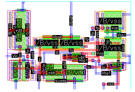
Selected block layouts
Five of six analog blocks reached block-level layout. Two representative layouts are shown here. Electrical results are labeled by evaluation method.
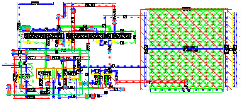
Bootstrapped switch
Block-level layout of the bootstrapped sampling switch.
Folded-cascode OTA
Block-level layout of the PMOS-input folded-cascode OTA for the 1.0 V design.
Simulation results
Targets and evaluation status
| Requirement | Result | Status and scope |
|---|---|---|
| SNDR ≥80 dB | 78.38 dB | Missed by 1.62 dB in the noise-included behavioral model |
| ENOB ≥12 bit | 12.73 bit | Met in the same behavioral evaluation |
| Power <50 µW | ≈46 µW partial | Full-chip target remains unverified |
| FoM <100 fJ/step | ≈136 fJ/step | Missed even with partial power and behavioral ENOB |
BEHAVIORAL · NOISE INCLUDED
78.38dB
calibrated behavioral model · 20 independent noise realizations
12.73 bitmean ENOB
78.05–78.81 dBnoise-realization range
1.62 dBbelow 80-dB target
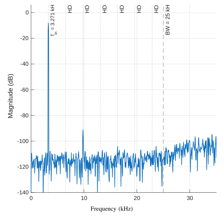
The 78.38-dB mean is 1.62 dB below the 80-dB target. What varies across the 20 evaluations is the random noise realization. This is not a process or mismatch Monte Carlo sweep. Mean ENOB is 12.73 bit.
Model boundary. The paper specifies a calibrated sampled/OTA-noise model with simplified finite-gain leakage, but does not identify its feedback-DAC level mapping. The result is not verified for the schematic’s ±437.5 mV DAC range. A model/configuration artifact is needed to establish that relationship.
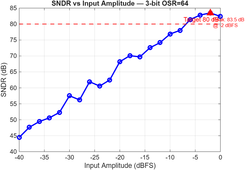
BEHAVIORAL REFERENCE · QUANTIZATION ONLY
83.5dB
idealized behavioral peak · −2 dBFS
Behavioral SNDR sweep
This sweep isolates quantization-noise shaping at OSReff = 64. The 83.5-dB peak is a reference-model result, not the final performance claim.
≈40 µW
VDD-powered core
+
6.25 µW
DAC ladders
=
≈46 µW
partial estimate
The ≈40 µW comes from closed-loop schematic VDD current. The two externally powered DAC strings add 6.25 µW, calculated from the nominal ladder values. Combining an approximate core value with that nominal contribution supports ≈46 µW, not full-chip power.
Block figures are separate checks: OTA core ≈2.3 µW per OTA and resistive CMFB ≈0.5 µW per OTA. Do not add these again to the VDD subtotal. The paper does not provide a complete per-block reconciliation. On-chip bias/reference generation, buffers, pads/ESD, decimation, and layout parasitics remain outside the estimate.
CLOSED-LOOP SCHEMATIC
Transient behavior
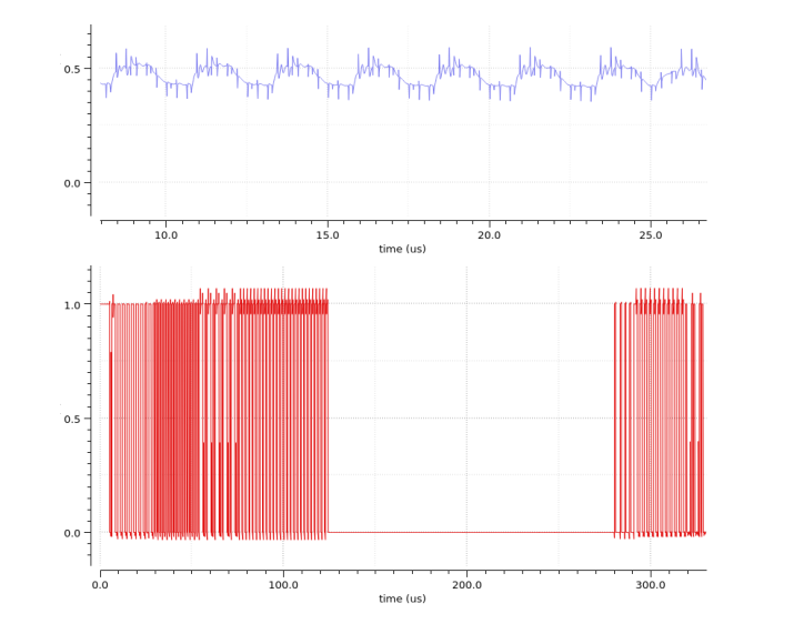
The schematic transient run checks bounded loop behavior over a finite interval. The plots show the first-integrator node V1p and B0, one bit of the 3-bit quantizer output. B0 alone does not establish decoded multibit tracking or spectral performance.
- V1p bounded7–27 µs detail stays around the common-mode operating region.
- One quantizer bit shownB0 switching activity over 330 µs. The complete 3-bit output word is not plotted here.
- No divergence observedIntegrator states remain bounded over the simulated interval.
Verification scope
Behavioral models, schematic simulations, and block-level drawings are separate evidence domains.
Evaluated
Behavioral SNDR and ENOB. OTA DC/AC. Closed-loop schematic transient behavior. Block-level layout drawings.
Outside current scope
Fabricated silicon. Full-system PEX/post-layout performance. Mismatch Monte Carlo. Transistor-level spectral SNDR.